ANR-Programme Nanotechnologies et Nanosystèmes – P2N – 2011

n°: ANR-11-NANO-012
Titre: Intégration de Nanofils III-V sur SOI pour COnnections Optiques sur Puce
Title: III-V nanowires integration on SOI for on-chip optical connections
5 Partners:
![]()
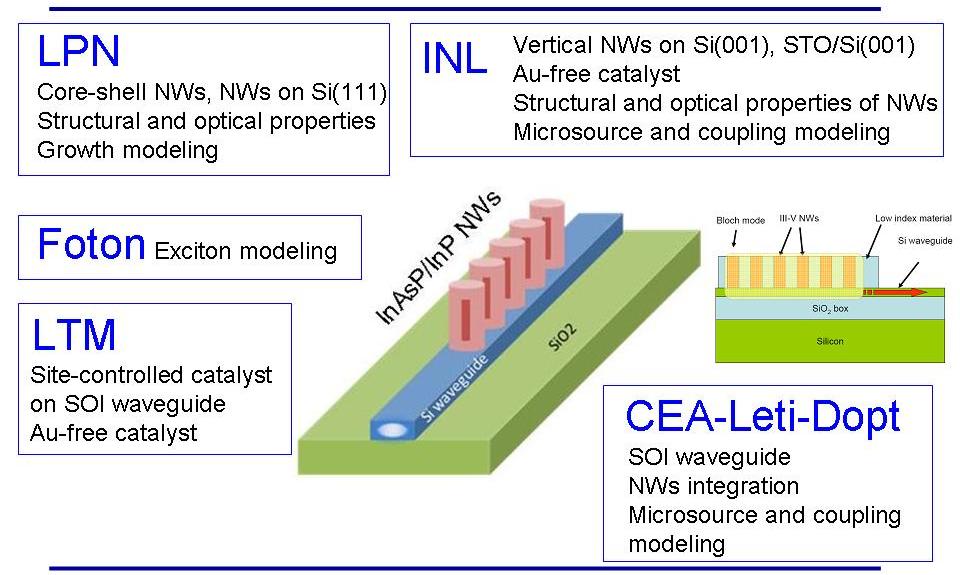
1- INL-Institut des Nanotechnologies de Lyon, UMR 5270
2- LPN-Laboratoire de Photonique et de Nanostructures, UPR 20
3- CEA-Leti-DOPT
4- LTM-Laboratoire des Technologies de la Microélectronique, UMR 5129
5- FOTON-INSA de Rennes
Organization
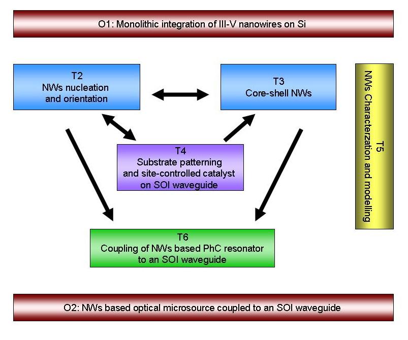
Coordinator: M. Gendry-INL for task T1 « Project management »
A scientific/technical manager will be indicated for the 5 scientific tasks of the project:
M. Gendry-INL for task T2: NW nucleation and orientation
J.C. Harmand-LPN for task T3: Core-shell NWs
B. Salem-LTM for task T4: Substrate patterning and site-controlled catalyst on an SOI waveguide
JM. Jancou-FOTON for task T5: Characterization and modelling of NW properties (transversal task)
B. Ben Bakir-CEA for task T6: Coupling of NWs-based PhC resonator to an SOI waveguide
Objective:
This project proposes an original strategy to integrate optical links on Si wafer for on-chip interconnects. The link consists of a Si optical waveguide fabricated from a SOI (Si on insulator) substrate. A compact optical source operating at 1.2 µm wavelength or above will be fabricated directly on the Si waveguide. This source is based on III-V materials deposited selectively on the Si surface in the form of vertical photonic wires standing on top of the waveguide. A regular array of such wires will form a resonant active photonic crystal. The project aims at demonstrating that under optical pumping, hybrid Bloch modes can be amplified in the III-V wire array and propagate in the passive Si waveguide. This demonstration will pave the way to fully integrated photonic links on Si chips.
For the sake of compatibility with CMOS technology, we propose to fabricate this device with a monolithic approach which can be implemented with high yield at large scale and high density, conversely to wafer bonding techniques. The integration of III-V material is based on epitaxial growth of nanowires (NWs) by the catalyst-assisted vapor-liquid-solid (VLS) method. This approach is very efficient to obtain defect-free materials of high optical quality, despite the highly mismatched interface between III-V and Si. Regular arrays will be obtained by patterning a SiO2 mask with nano-sized openings containing the catalyst particles. Core-shell heterostructures will be formed to limit carrier surface recombination. We will focus on the InAsP/InP system which covers the targeted wavelengths for which Si is transparent. Core and shell will be formed with adequate dimensions in successive growth steps. The full compatibility with CMOS raises critical issues which are addressed in the project. Growth must be performed on (001) oriented Si surface and without Au as catalyst which is an impurity to be avoided in CMOS process lines. We rely on the experience of one partner as well as on the recent literature to investigate alternative catalysts. On (001) surfaces, VLS process results in inclined NWs growing along the <111> directions of the substrate. To get vertically standing NWs on Si(001), a very thin intermediate layer of SrTiO3 is proposed on the basis of preliminary results of one partner. These growth and patterning issues are addressed in tasks 2, 3 and 4 of the project.
The former activities will be supported by task 5 dealing with material structural and optical characterization and modeling. Modeling tools will be developed to optimize the VLS growth conditions. Of particular importance for the project, the conditions which stabilize the NW crystalline phase will be predicted for the self-catalytic case. Tight-binding and k.p models will be implemented to calculate the electronic properties of NWs with core-shell heterostructures of wurzite phase. These calculations, not yet available in the literature, will evaluate the excitonic and piezo-electric effects of major importance for the efficiency of the optical source.
Task 6 will be dedicated to the optimization and evaluation of the optical micro-source (resonant LED or lasers). Electromagnetic simulations will guide the design of the periodic array of III-V photonic NWs on Si. High quality factor resonances and efficient coupling between these micro-resonators and the SOI waveguide will be targeted. After the fabrication of the NW arrays, their planarization with a low-index insulating material will be tested. This technological step will anticipate a longer term objective (out of the scope of this project), i.e. electrically injected devices. The emission characteristics of the micro-source will be measured under optical pumping, with and without device planarization. This ultra-compact source of original architecture is expected to have enhanced global efficiency and reduced power consumption, which is of prime importance in the field of silicon photonics.